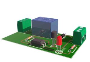
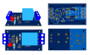
PCB isolated relay module
This is the PCB design of this circuit . It’s a two layer PCB with the thickness of 1mm.The PCB has two sections . One is the AC side the other is the DC side both are separated in the PCB design to prevent any damage in case of a leak. You can upload this files directly to a PCB manufacturing site such as JLPCB and made your own PCB . The zip file include Gerber file , BOM file and Pick and place file . You can download the file form HERE !